TI 公司的ECG解决方案是采用TMS320VC5505 定点DSP,它是基于TMS320C55x DSP CPU核的定点DSP,它的C55x? DSP架构可得到高性能和低功耗特性,CPU支持内部总线架构,包括一条可编程总线,一条321位数据总总线和两条16位数据读总线,两条数据写总线和专门用于外设和DMA的其它总线. TMS320VC5505还包括4个DMA控制器,每个四路.时钟为60MHz或100MHz,指令周期为16.67ns或10ns.主要用于无线音频设备,回声消除耳机,手提媒体设备,视频,工业控制,指纹生物学和SDR. 本文介绍了TMS320VC5505的主要特性和方框图以及采用TMS320VC5505的ECG解决方案方框图, ECG前端板详细电路图和所用材料清单(BOM).
Basic functions of an ECG machine include ECG waveform display, either through LCD screen or printed paper media, and heart rhythm indication as well as simple user interface through buttons. More features, such as patient record storage through convenient media, wireless/wired transfer and 2D/3D display on large LCD screen with touch screen capabilities, are required in more and more ECG products. Multiple levels of diagnostic capabilities are also assisting doctors and people without specific ECG trainings to understand ECG patterns and their indication of a certain heart condition. After the ECG signal is captured and digitized, it will be sent for display and analysis, which involves further signal processing.
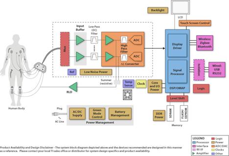
图1。TI ECG方框图
ECG Implementation on the TMS320VC5505 DSP Medical Development Kit (Rev. A)
The TMS320VC5505 is a member of TIs TMS320C5000? fixed-point Digital Signal Processor (DSP) product family and is designed for low-power applications.
The TMS320VC5505 fixed-point DSP is based on the TMS320C55x? DSP generation CPU processor core. The C55x? DSP architecture achieves high performance and low power through increased parallelism and total focus on power savings. The CPU supports an internal bus structure that is composed of one program bus, one 32-bit data read bus and two 16-bit data read buses, two 16-bit data write buses, and additional buses dedicated to peripheral and DMA activity. These buses provide the ability to perform up to four 16-bit data reads and two 16-bit data writes in a single cycle. The TMS320VC5505 also includes four DMA controllers, each with 4 channels, providing data movements for 16-independent channel contexts without CPU intervention. Each DMA controller can perform one 32-bit data transfer per cycle, in parallel and independent of the CPU activity.
The C55x CPU provides two multiply-accumulate (MAC) units, each capable of 17-bit x 17-bit multiplication and a 32-bit add in a single cycle. A central 40-bit arithmetic/logic unit (ALU) is supported by an additional 16-bit ALU. Use of the ALUs is under instruction set control, providing the ability to optimize parallel activity and power consumption. These resources are managed in the Address Unit (AU) and Data Unit (DU) of the C55x CPU.
The C55x CPU supports a variable byte width instruction set for improved code density. The Instruction Unit (IU) performs 32-bit program fetches from internal or external memory and queues instructions for the Program Unit (PU). The Program Unit decodes the instructions, directs tasks to the Address Unit (AU) and Data Unit (DU) resources, and manages the fully protected pipeline. Predictive branching capability avoids pipeline flushes on execution of conditional instructions.
The general-purpose input and output functions along with the 10-bit SAR ADC provide sufficient pins for status, interrupts, and bit I/O for LCD displays, keyboards, and media interfaces. Serial media is supported through two MultiMedia Card/Secure Digital (MMC/SD) peripherals, four Inter-IC Sound (I2S Bus?) modules, one Serial-Port Interface (SPI) with up to 4 chip selects, one I2C multi-master and slave interface, and a Universal Asynchronous Receiver/Transmitter (UART) interface.
The VC5505 peripheral set includes an external memory interface (EMIF) that provides glueless access to asynchronous memories like EPROM, NOR, NAND, and SRAM. Additional peripherals include: a high-speed Universal Serial Bus (USB2.0) device mode only, and a real-time clock (RTC). The DMA controller provides data movement for sixteen independent channel contexts without CPU intervention, providing DMA throughput of up to two 16-bit words per cycle. This device also includesthree general-purpose timers with one configurable as a watchdog timer, and a analog phase-locked loop (APLL) clock generator.
In addition, the VC5505 includes a tightly-coupled FFT Hardware Accelerator. The tightly-coupled FFT Hardware Accelerator supports 8 to 1024-point (in power of 2) real and complex-valued FFTs.
TMS320VC5505主要特性:
High-Performance, Low-Power, TMS320C55x? Fixed-Point Digital Signal Processor
16.67-, 10-ns Instruction Cycle Time 60-, 100-MHz Clock Rate
One/Two Instruction(s) Executed per Cycle
Dual Multipliers [Up to 200 Million Multiply-Accumulates per Second (MMACS)]
Two Arithmetic/Logic Units (ALUs)
Three Internal Data/Operand Read Buses and Two Internal Data/Operand Write Buses
Fully Software-Compatible With C55x Devices
Industrial Temperature Devices Available
320K Bytes Zero-Wait State On-Chip RAM, Composed of:
64K Bytes of Dual-Access RAM (DARAM), 8 Blocks of 4K x 16-Bit
256K Bytes of Single-Access RAM (SARAM), 32 Blocks of 4K x 16-Bit
128K Bytes of Zero Wait-State On-Chip ROM (4 Blocks of 16K x 16-Bit)
16-/8-Bit External Memory Interface (EMIF) with Glueless Interface to:
8-/16-Bit NAND Flash, 1- and 4-Bit ECC
8-/16-Bit NOR Flash
Asynchronous Static RAM (SRAM)
Direct Memory Access (DMA) Controller Four DMA With 4 Channels Each (16-Channels Total)
Three 32-Bit General-Purpose Timers
One Selectable as a Watchdog and/or GP
Two MultiMedia Card/Secure Digital (MMC/SD) Interfaces
Universal Asynchronous Receiver/Transmitter (UART)
Serial-Port Interface (SPI) With Four Chip-Selects
Master/Slave Inter-Integrated Circuit (I2C Bus?)
Four Inter-IC Sound (I2S Bus?) for Data Transport
Device USB Port With Integrated 2.0 High-Speed PHY that Supports: USB 2.0 Full- and High-Speed Device
LCD Bridge With Asynchronous Interface
Tightly-Coupled FFT Hardware Accelerator
10-Bit 4-Input Successive Approximation (SAR) ADC
Real-Time Clock (RTC) With Crystal Input, With Separate Clock Domain, Separate Power Supply
Four Core Isolated Power Supply Domains: Analog, RTC, CPU and Peripherals, and USB
Four I/O Isolated Power Supply Domains: RTC I/O, EMIF I/O, USB PHY, and DVDDIO
Low-Power S/W Programmable Phase-Locked Loop (PLL) Clock Generator
On-Chip ROM Bootloader (RBL) to Boot From NAND Flash, NOR Flash, SPI EEPROM, or I2C EEPROM
IEEE-1149.1 (JTAG?) Boundary-Scan-Compatible
Up to 26 General-Purpose I/O (GPIO) Pins (Multiplexed With Other Device Functions)
196-Terminal Pb-Free Plastic BGA (Ball Grid Array) (ZCH Suffix)
1.05-V Core (60 MHz), 1.8-V, 2.5-V, 2.8-V, or 3.3-V I/Os
1.3-V Core (100 MHz), 1.8-V, 2.5-V, 2.8-V, or 3.3-V I/Os
TMS320VC5505应用:
Wireless Audio Devices (e。g。, Headsets, Microphones, Speakerphones, etc.)
Echo Cancellation Headphones
Portable Medical Devices
Voice Applications
Industrial Controls
Fingerprint Biometrics
Software Defined Radio

图2。TMS320VC5505功能方框图
A number of emerging medical applications such as electrocardiography (ECG), digital stethoscope, and pulse oximeters require DSP processing performance at very low power. The TMS320VC5505 digital signal processor (DSP) is ideally suited for such applications. The VC5505 is a member of TIs C5000? fixed-point DSP platform. To enable the development of a broad range of medical applications on the VC5505, Texas Instruments has developed an MDK based on the VC5505 DSP. A typical medical application includes:
An analog front end, including sensors to pick up signals of interest from the body
Signal processing algorithms for signal conditioning, performing measurements and running analytics on measurements to determine the health condition
User control and interaction, including graphical display of the signal processing results and connectivity to enable remote patient monitoring
The MDK is designed to support complete medical applications development. It includes the following elements:
Analog front-end boards (FE boards) specific to the key target medical applications of the VC5505 (ECG, digital stethoscope, pulse oximeter), highlighting the use of the TI analog components for medical applications
VC5505 DSP evaluation module (EVM) main board
Medical applications software including example demonstrations Several elements of the MDK pulse oximeter system are:
VC5505 EVM
Pulse oximeter front-end board
Finger probe sensor
The schematics for the ECG front-end board

图3. ECG前端板电路图(1)

图4. ECG前端板电路图(2): ECG电极:V1 V2 V3

图5. ECG前端板电路图(3):ECG电极:V4 V5 V6

图6. ECG前端板电路图(4):ADC部分
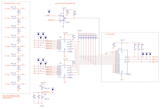
图7. ECG前端板电路图(5):ECG电极检测

图8. ECG前端板电路图(6):右腿驱动部分

图9. ECG前端板电路图(7):电源和接口部分
ECG前端板材料清单:


详情请见:
http://focus.ti.com/lit/ds/symlink/tms320vc5505.pdf
和
http://focus.ti.com/lit/an/sprab36a/sprab36a.pdf